- 您现在的位置:买卖IC网 > Sheet目录2007 > MAX11046ECB+T (Maxim Integrated Products)IC ADC 16BIT PAR 250KSPS 64TQFP
4-/6-/8-Channel, 16-/14-Bit,
Simultaneous-Sampling ADCs
15
Maxim Integrated
MAX11044/MAX11044B/MAX11045/MAX11045B/
MAX11046/MAX11046B/MAX11054/MAX11055/MAX11056
Detailed Description
The MAX11044/MAX11044B/MAX11045/MAX11045B/
MAX11046/MAX11046B and MAX11054/ MAX11055/
MAX11056 are fast, low-power ADCs that combine 4, 6, or 8
independent ADC channels in a single IC. Each channel
includes simultaneously sampling independent T/H circuitry
that preserves relative phase information between inputs
making
the
MAX11044/MAX11044B/MAX11045/
MAX11045B/MAX11046/MAX11046B and MAX11054/
MAX11055/MAX11056 ideal for motor control and power
monitoring. The MAX11044/MAX11044B/MAX11045/
MAX11045B/MAX11046/MAX11046B and MAX11054/
MAX11055/MAX11056 are available with ±5V input
ranges that feature ±20mA overrange, fault-tolerant inputs.
The MAX11044/MAX11044B/MAX11045/MAX11045B/
MAX11046/MAX11046B and MAX11054/MAX11055/
MAX11056 operate with a single 4.75V to 5.25V supply. A
separate 2.7V to 5.25V supply for digital circuitry makes
the devices compatible with low-voltage processors.
The MAX11044/MAX11044B/MAX11045/MAX11045B/
MAX11046/MAX11046B and MAX11054/MAX11055/
MAX11056 perform conversions for all channels in par-
allel by activating independent ADCs. Results are avail-
able through a high-speed, 20MHz, parallel data bus
after a conversion time of 3μs following the end of a
sample. The data bus is bidirectional and allows for
easy programming of the configuration register. The
MAX11044/MAX11044B/MAX11045/MAX11045B/
MAX11046/MAX11046B and MAX11054/MAX11055/
MAX11056 feature a reference buffer, which is driven by
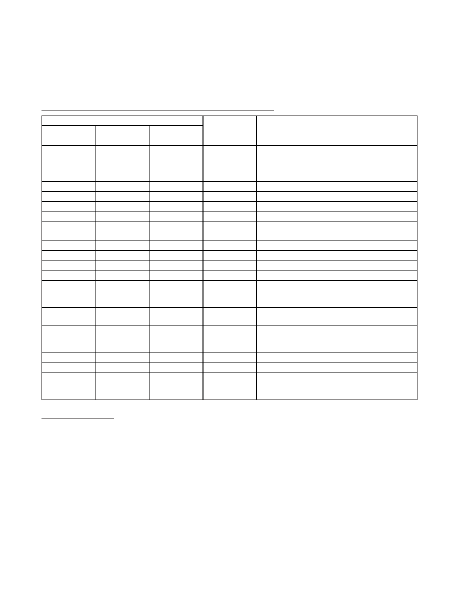
Pin Description (continued)
PIN
MAX11054
(TQFP-EP)
MAX11055
(TQFP-EP)
MAX11056
(TQFP-EP)
NAME
FUNCTION
27, 33, 40, 48,
54
27, 33, 40, 48,
54
27, 33, 40, 48,
54
RDC
Reference Buffer Decoupling. Connect all RDC outputs
together. Bypass to AGND with at least an 80μF total
capacitance. See the Layout, Grounding, and Bypassing
section.
37
34
31
CH0
Channel 0 Analog Input
39
37
34
CH1
Channel 1 Analog Input
42
39
37
CH2
Channel 2 Analog Input
44
42
39
CH3
Channel 3 Analog Input
41
REFIO
External Reference Input/Internal Reference Output.
Place a 0.1μF capacitor from REFIO to AGND.
—
44
42
CH4
Channel 4 Analog Input
—
47
44
CH5
Channel 5 Analog Input
—
47
CH6
Channel 6 Analog Input
—
50
CH7
Channel 7 Analog Input
61
WR
Active-Low Write Input. Drive WR low to write to the
ADC. Configuration registers are loaded on the rising
edge of WR.
62
CS
Active-Low Chip-Select Input. Drive CS low when
reading from or writing to the ADC.
63
RD
Active-Low Read Input. Drive RD low to read from the
ADC. Each rising edge of RD advances the channel
output on the data bus.
64
DB13
14-Bit Parallel Data Bus Digital Output Bit 13
31, 34, 47, 50
31, 50
—
I.C.
Internally Connected. Connect to AGND.
———
EP
Exposed Pad. Internally connected to AGND. Connect to
a large ground plane to maximize thermal performance.
Not intended as an electrical connection point.
发布紧急采购,3分钟左右您将得到回复。
相关PDF资料
MAX11046ETN+T
ADC 16BIT SAMPLING 8CH 56-TQFN
MAX11049ECB+
IC ADC 16BIT PAR 250KSPS 64TQFP
MAX1104EUA+
IC CODEC 8BIT 8-UMAX
MAX11100EUB+
IC ADC 16BIT SRL 200KSPS 10UMAX
MAX11101EUB+
IC ADC 14BIT SRL 200KSPS 10UMAX
MAX11102AUB+
IC ADC 12BIT SPI/SRL 10UMAX-EP
MAX1111CPE+
IC ADC 8BIT LP 16-DIP
MAX1113CPE+
IC ADC 8BIT LP 16-DIP
相关代理商/技术参数
MAX11046ECB+TW
功能描述:模数转换器 - ADC 16-Bit Simultaneous Sampling ADC RoHS:否 制造商:Texas Instruments 通道数量:2 结构:Sigma-Delta 转换速率:125 SPs to 8 KSPs 分辨率:24 bit 输入类型:Differential 信噪比:107 dB 接口类型:SPI 工作电源电压:1.7 V to 3.6 V, 2.7 V to 5.25 V 最大工作温度:+ 85 C 安装风格:SMD/SMT 封装 / 箱体:VQFN-32
MAX11046ECB+W
功能描述:模数转换器 - ADC 16-Bit Simultaneous Sampling ADC RoHS:否 制造商:Texas Instruments 通道数量:2 结构:Sigma-Delta 转换速率:125 SPs to 8 KSPs 分辨率:24 bit 输入类型:Differential 信噪比:107 dB 接口类型:SPI 工作电源电压:1.7 V to 3.6 V, 2.7 V to 5.25 V 最大工作温度:+ 85 C 安装风格:SMD/SMT 封装 / 箱体:VQFN-32
MAX11046ETN+
功能描述:模数转换器 - ADC 16Bit 8Ch Simult Sampling
RoHS:否 制造商:Texas Instruments 通道数量:2 结构:Sigma-Delta 转换速率:125 SPs to 8 KSPs 分辨率:24 bit 输入类型:Differential 信噪比:107 dB 接口类型:SPI 工作电源电压:1.7 V to 3.6 V, 2.7 V to 5.25 V 最大工作温度:+ 85 C 安装风格:SMD/SMT 封装 / 箱体:VQFN-32
MAX11046ETN+
制造商:Maxim Integrated Products 功能描述:IC ADC 16BIT 250KSPS TQFN-56
MAX11046ETN+T
功能描述:模数转换器 - ADC 16Bit 8Ch Simult Sampling RoHS:否 制造商:Texas Instruments 通道数量:2 结构:Sigma-Delta 转换速率:125 SPs to 8 KSPs 分辨率:24 bit 输入类型:Differential 信噪比:107 dB 接口类型:SPI 工作电源电压:1.7 V to 3.6 V, 2.7 V to 5.25 V 最大工作温度:+ 85 C 安装风格:SMD/SMT 封装 / 箱体:VQFN-32
MAX11046ETN+TW
功能描述:模数转换器 - ADC 16-Bit Simultaneous Sampling ADC RoHS:否 制造商:Texas Instruments 通道数量:2 结构:Sigma-Delta 转换速率:125 SPs to 8 KSPs 分辨率:24 bit 输入类型:Differential 信噪比:107 dB 接口类型:SPI 工作电源电压:1.7 V to 3.6 V, 2.7 V to 5.25 V 最大工作温度:+ 85 C 安装风格:SMD/SMT 封装 / 箱体:VQFN-32
MAX11046ETN+W
功能描述:模数转换器 - ADC 16-Bit Simultaneous Sampling ADC RoHS:否 制造商:Texas Instruments 通道数量:2 结构:Sigma-Delta 转换速率:125 SPs to 8 KSPs 分辨率:24 bit 输入类型:Differential 信噪比:107 dB 接口类型:SPI 工作电源电压:1.7 V to 3.6 V, 2.7 V to 5.25 V 最大工作温度:+ 85 C 安装风格:SMD/SMT 封装 / 箱体:VQFN-32
MAX11046EVKIT+
功能描述:数据转换 IC 开发工具 MAX11046 Eval Kit
RoHS:否 制造商:Texas Instruments 产品:Demonstration Kits 类型:ADC 工具用于评估:ADS130E08 接口类型:SPI 工作电源电压:- 6 V to + 6 V